The frequency converters of the German manufacturer Lenze are designed for mass use, for those applications where motors already need regulation, but there are no inexpensive and practical solutions yet. Lenze just filled this part of the market. Just one example is enough: the pipeline. This is a mechanism that should smoothly pick up speed and smoothly stop.
Until now, he required either complex kinematics or a drive direct current, or had to put up with his sharp jolts. The use of a Lenze frequency converter completely solves the problem. With a simple mechanism, it is easy to provide high performance machines in a wide range of capacities. All you have to do is set up the converter.
Work principles
In previous years, the circuitry of frequency converters did not allow such opportunities as are available today. Modern ones contain a single- or three-phase rectifier at the input (single-phase for low power models), then a capacitive filter, and at the output a three-phase bridge on the keys.
These switches make it possible to switch significant currents with a high modulating frequency, forming sinusoids with frequencies from almost 0 to hundreds of Hz. Theoretically, this makes it possible to spin asynchronous motors up to 6000 rpm, but in practice 2-3 times. It is possible to carry out, including long-term, if external braking resistors for braking current are connected.
The smd series inverters are designed for conventional linear or quadratic V/f control, while the tmd series uses vector control.
Characteristics of the Lenze 8200 SMD converter
It is designed to work with asynchronous motors in a wide power range. This product has been designed to control a drive with a linear or quadratic function. The inverter does not use vector control.
Figure: Lenze smd schematic.
For the vast majority of simple operations with low and low power motors under light loads, this is not required. Much more valued are: ease of setup, ease of maintenance, small dimensions of the converter. Lenze smd offers all this to its consumer in full:
- speed control;
- change of direction of rotation;
- separate adjustment of acceleration and braking;
- protection and security;
- small weight and dimensions;
- possibility of overload by 1.5 times up to one minute.
Characteristics of the Lenze 8200 TMD converter
This converter is designed to work with asynchronous motors installed in mechanisms where vector or torque control is preferred.
Instructions for launching QIANGLI SMD modules (chip 16188B) on Onbon BX controllers
Recently, the QIANGLI factory has begun to produce new LED modules P10 Red SMD, and many failed to run the running lines built on these modules. The reason for this failure turned out to be very simple - the factory installed a new 16188B chip, with which the controllers refused to work without special firmware. Controller manufacturers rapidly began to develop firmware for this chip, and now we will tell you where to get the firmware and how to flash the controller.
On the this moment series controllers can work with red SMD modules:
BX-5U, BX-5A, BX-5M. For controllers BX-5UL/UT/U0/U1/U2, BX-5MT/M1/M2, BX-5AT/A0/A1/A2, a prerequisite is the presence of a central chip “6U” (controllers with a 5U chip cannot be flashed). Controllers BX-5U3/U4, BX-5M3/M4, BX-5A4 have a more powerful 5U chip on board and can be flashed. Unfortunately, other controllers of the fifth series and controllers of the BX-6E series still cannot work with these modules.
First you need to download the very firmware that allows the controller to work with the 16188B chip.
On our website in the section, you will always find the latest firmware versions, both conventional and special for a particular chip. After going to the section for downloading the file, click on the series of controllers that you plan to use. In the list that appears, you need to download the firmware, in which the 16188B chip is registered in the description and name.

After the download is complete, extract the contents of the archive to any place convenient for you, for example, to your desktop.
Launch LedshowTW. Go to the "Settings" tab, "Screen settings settings", in the window that appears, enter the password 888. Select the series and type of controller that you plan to use. At this stage, it is not necessary to enter all the data of the ticker, now it is necessary that the program understand which controller will be flashed, otherwise the program will either not allow the firmware to be updated (in the case of a direct connection via Lan or WiFi) or save the firmware, but the controller will not accept it, because .to. controller name verification will work and if it does not match, the controller will ignore the firmware file.
After selecting the type of controller, go to the "Settings", "Firmware maintenance" tab, in the window that appears, enter the password 888.
After the Firmware Maintenance window opens, click on the icon of the folder that opens.
Navigate to the directory where you extracted the firmware files and select the desired firmware. For example, to flash the BX-5M1 controller, you need to select the firmware "BX-5M1-/Firmware Version/.REL"

Note that the controller you want to update is selected in the Controller Type field. The font color should be black, if it is red, then you have selected the wrong firmware.
We have already got acquainted with the main radio components: resistors, capacitors, diodes, transistors, microcircuits, etc., and also studied how they are mounted on a printed circuit board. Once again, let's recall the main stages of this process: the leads of all components are passed into the holes available in the printed circuit board. After that, the conclusions are cut off, and then with reverse side boards are soldered (see Fig. 1).
This process already known to us is called DIP editing. This installation is very convenient for beginner radio amateurs: the components are large, you can solder them even with a large “Soviet” soldering iron without the help of a magnifying glass or microscope. That is why all Master Kits for self-soldering involve DIP mounting.
Rice. 1. DIP mounting
But DIP editing has very significant disadvantages:
Large radio components are not suitable for creating modern miniature electronic devices;
- output radio components are more expensive to manufacture;
- PCB for DIP-mounting is also more expensive due to the need to drill many holes;
- DIP mounting is difficult to automate: in most cases, even in large electronics factories, installation and soldering of DIP parts must be done manually. It is very expensive and time consuming.
Therefore, DIP-mounting during production modern electronics practically not used, and it was replaced by the so-called SMD process, which is the standard of today. Therefore, any radio amateur should have at least a general idea about it.
SMD mounting
SMD components (chip components) are components electronic circuit printed on a printed circuit board using surface mount technology - SMT technology (eng. surface mount technology). That is, all electronic elements that are “fixed” on the board in this way are called smd components(English) surface mounted device). The process of mounting and soldering chip components is properly called the SMT process. It is not entirely correct to say “SMD-assembly”, but in Russia this version of the name of the technical process has taken root, so we will say the same.
On fig. 2. shows a section of the SMD mounting board. The same board, made on DIP-elements, will have several times larger dimensions.

Fig.2. SMD mounting
SMD mounting has undeniable advantages:
Radio components are cheap to manufacture and can be arbitrarily miniature;
- printed circuit boards are also cheaper due to the lack of multiple drilling;
- installation is easy to automate: installation and soldering of components is carried out by special robots. There is also no such technological operation as trimming the leads.
SMD resistors
Acquaintance with chip components is most logical to start with resistors, as with the simplest and most massive radio components.
The SMD resistor in terms of its physical properties is similar to the “usual”, output version we have already studied. All of it physical parameters(resistance, accuracy, power) are exactly the same, only the case is different. The same rule applies to all other SMD components.

Rice. 3. CHIP resistors
Sizes of SMD resistors
We already know that output resistors have a certain grid of standard sizes, depending on their power: 0.125W, 0.25W, 0.5W, 1W, etc.
Chip resistors also have a standard size grid, only in this case the size is indicated by a four-digit code: 0402, 0603, 0805, 1206, etc.
The main sizes of resistors and their specifications shown in Fig.4.

Rice. 4 Main sizes and parameters of chip resistors
SMD marking-resistors
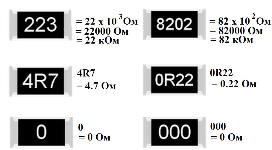
Resistors are marked with a code on the case.
If there are three or four digits in the code, then the last digit means the number of zeros, in fig. 5. The resistor with the code "223" has the following resistance: 22 (and three zeros on the right) Ohm = 22000 Ohm = 22 kOhm. The resistor with the code "8202" has a resistance: 820 (and two zeros on the right) Ohm = 82000 Ohm = 82 kOhm.
In some cases, the marking is alphanumeric. For example, a resistor coded 4R7 has a resistance of 4.7 ohms, and a resistor coded 0R22 has a resistance of 0.22 ohms (here, the letter R is the separator character).
There are also resistors of zero resistance, or jumper resistors. Often they are used as fuses.
Of course, you can not remember the code designation system, but simply measure the resistance of the resistor with a multimeter.
Rice. 5 Marking chip resistors
Ceramic SMD Capacitors
Externally, SMD capacitors are very similar to resistors (see Fig. 6.). There is only one problem: the capacitance code is not applied to them, so the only way to determine it is to measure it with a multimeter that has a capacitance measurement mode.
SMD capacitors are also available in standard sizes, usually similar to resistor sizes (see above).

Rice. 6. SMD ceramic capacitors
Electrolytic SMS Capacitors

Fig.7. Electrolytic SMS Capacitors
These capacitors are similar to their output counterparts, and the markings on them are usually explicit: capacitance and operating voltage. A strip on the "hat" of the capacitor marks its negative terminal.
SMD transistors

Fig.8. SMD transistor
Transistors are small, so it is impossible to write their full name on them. They are limited to code marking, and there is no international standard for designations. For example, the code 1E may indicate the type of transistor BC847A, or maybe some other. But this circumstance absolutely does not bother either manufacturers or ordinary consumers of electronics. Difficulties can only arise during repairs. Determining the type of transistor installed on a printed circuit board without the manufacturer's documentation for this board can sometimes be very difficult.
SMD Diodes and SMD LEDs
Photos of some diodes are shown in the figure below:

Fig.9. SMD Diodes and SMD LEDs
On the body of the diode, the polarity must be indicated in the form of a strip closer to one of the edges. Usually the cathode output is marked with a stripe.
The SMD LED also has a polarity, which is indicated either by a dot near one of the pins, or in some other way (you can find out more about this in the component manufacturer's documentation).
It is difficult to determine the type of SMD diode or LED, as in the case of a transistor: an uninformative code is stamped on the diode case, and most often there are no marks on the LED case at all, except for the polarity mark. Developers and manufacturers of modern electronics care little about its maintainability. It is understood that the repair of the printed circuit board will be a service engineer who has complete documentation for a particular product. Such documentation clearly describes where a particular component is installed on the printed circuit board.
Installation and soldering of SMD components
SMD assembly is optimized primarily for automatic assembly by special industrial robots. But amateur radio amateur designs can also be made on chip components: with sufficient accuracy and care, you can solder parts the size of a grain of rice with the most ordinary soldering iron, you only need to know some subtleties.
But this is a topic for a separate large lesson, so more details about automatic and manual SMD editing will be discussed separately.
Good soldering, although not as important as the correct placement of radio elements, but it also plays a significant role. Therefore, we will consider SMD installation - what is needed for it and how it should be done at home.
Stocking up and preparing
For quality work, we need to have:
- Solder.
- Tweezers or pliers.
- Soldering iron.
- A small sponge.
- Side cutters.
First you need to plug in the soldering iron. Then dampen the sponge with water. When the soldering iron is heated to such an extent that it can melt the solder, then it is necessary to cover the tip with it (solder). Then wipe it with a damp sponge. At the same time, too long contact should be avoided, as it is fraught with hypothermia. To remove the remnants of old solder, you can wipe the tip on a sponge (and also to keep it clean). Preparation is also carried out in relation to the radio component. Everything is done with tweezers or pliers. To do this, it is necessary to bend the leads of the radio component so that they can easily enter the holes in the board. Now let's talk about how SMD components are mounted.
Getting Started with Parts
Initially, you need to insert the components into the holes on the board that are intended for them. When doing this, make sure that the polarity is observed. This is especially important for elements such as electrolytic capacitors and diodes. Then you should slightly spread the leads so that the part does not fall out of the established place (but do not overdo it). Just before you start soldering, do not forget to wipe the tip with a sponge again. Now let's look at how SMD is installed at home at the soldering stage.
Fixing details

It is necessary to place the tip of the soldering iron between the board and the output in order to warm up the place where the soldering will be carried out. In order not to disable the part, this time should not exceed 1-2 seconds. Then you can bring solder to the place of soldering. Keep in mind that at this stage flux can splash on a person, so be careful. After the moment when the required amount of solder has time to melt, it is necessary to take the wire away from the place where the part is soldered. For its uniform distribution, it is necessary to hold the soldering iron tip for a second. Then, without moving the part, it is necessary to remove the device. It will take a few moments, and the place of soldering will cool down. All this time it is necessary to ensure that the part does not change its location. Excess can be cut off using side cutters. But make sure that the soldering point is not damaged.
Checking the quality of work

Look at the resulting SMD surface mount:
- Ideally, the contact area and part lead should be connected. In this case, the soldering itself should have a smooth and shiny surface.
- If a spherical shape is obtained or if there is a connection with neighboring pads, it is necessary to heat up the solder and remove its excess. Keep in mind that after working with it, there is always a certain amount of it on the soldering iron tip.
- If there is a matte surface and scratches, melt the solder again and, without moving the parts, let it cool. If necessary, you can add it in a small amount.
A suitable solvent can be used to remove flux residue from the board. But this operation is not mandatory, because its presence does not interfere and does not affect the functioning of the circuit. And now let's pay attention to soldering theory. Then we will go through the features of each individual option.
Theory

Soldering is understood as the connection of certain metals with the use of other, more fusible ones. In electronics, solder is used for this, in which 40% lead and 60% tin. This alloy becomes liquid already at 180 degrees. Modern solders are produced as thin tubes that are already filled with a special resin that acts as a flux. Heated solder can create an internal connection if the following conditions are met:
- It is necessary that the surfaces of the parts to be soldered be cleaned. To do this, it is important to remove all oxide films that form over time.
- The part must be heated at the place of soldering to a temperature that is sufficient to melt the solder. Certain difficulties arise here when there is a large area with good thermal conductivity. After all, elementary power of the soldering iron may not be enough to heat the place.
- Care must be taken to protect against oxygen. This task can be performed by colophonium, which forms a protective film.
Most Common Mistakes

Now let's look at three of the most common mistakes and how to fix them:
- The soldering points are touched with the tip of the soldering iron tip. In this case, too little heat is supplied. It is necessary to apply the tip in such a way that the largest contact area is created between the tip and the soldering point. Then SMD installation will turn out to be of high quality.
- Too little solder is used and long periods of time are maintained. When the process itself begins, part of the flux has already evaporated. The solder does not receive a protective layer, as a result - an oxide film. And how to properly install SMD at home? To do this, soldering professionals pump both the soldering iron and the solder at the same time.
- Too early retraction of the tip from the soldering point. Heat up intensely and quickly.
You can take a capacitor for SMD mounting and fill your hand on it.
Soldering loose wires
Now we are going to practice. Let's say we have an LED and a resistor. You need to solder a cable to them. It does not use mounting plates, pins and other auxiliary elements. To achieve this goal, you need to perform the following operations:
- Remove the insulation from the ends of the wire. They must be clean as they have been protected from moisture and oxygen.
- We twist the individual wires of the core. This prevents their subsequent loosening.
- We tin the ends of the wires. During this process, it is necessary to bring the heated tip to the wire along with the solder (which should be evenly distributed over the surface).
- We shorten the leads of the resistor and LED. Then you need to tin them (regardless of whether old or new parts are used).
- Hold the leads parallel and apply a small amount of solder. As soon as the gaps are evenly filled with it, it is necessary to quickly withdraw the soldering iron. Until the solder hardens completely, the part does not need to be touched. If this nevertheless happened, then microcracks appear, which adversely affect the mechanical and electrical properties of the connection.
PCB Soldering

In this case, it is necessary to apply less effort than in the previous one, since here the board holes play a good role as a retainer for parts. But experience is also important here. Often the result of the work of beginners is that the circuit begins to look like one large and solid conductor. But this is a simple matter, so after a little training, the result will be at a decent level.
Now let's figure out how SMD mounting works in this case. Initially, the tip of the soldering iron and solder are simultaneously brought to the place of soldering. Moreover, both the processed conclusions and the board should heat up. It is necessary to hold the sting until the solder evenly covers the entire contact point. Then it can be circled in a semicircle around the treated area. In this case, the solder should move in the opposite direction. We observe that it is evenly distributed over the entire contact area. After that, remove the solder. And the last step is to quickly remove the tip from the place of soldering. We are waiting for the solder to acquire its final shape and harden. This is how the SMD is mounted in this case. at the first attempts, it will not look so hot, but over time you can learn how to do it at such a level that you can’t distinguish it from the factory version.
- Introduction
- SMD Component Enclosures
- Sizes of SMD components
- SMD resistors
- SMD Capacitors
- SMD coils and chokes
- SMD transistors
- Marking SMD components
- Soldering SMD components
Introduction
Not only ordinary components with leads are now available to a modern radio amateur, but also such small, dark ones, on which one cannot understand what is written, details. They are called "SMD". In Russian it means "surface mount components". Their main advantage is that they allow the industry to assemble boards using robots that place SMD components at great speed in their places on printed circuit boards, and then massively “bake” and receive assembled printed circuit boards as a result. On the part of the person are those operations that the robot cannot perform. Not yet.
The use of chip components in amateur radio practice is also possible, even necessary, as it allows to reduce the weight, size and cost of the finished product. Plus, you don't have to drill at all.
For those who first encountered SMD components, confusion is natural. How to understand their diversity: where is the resistor, and where is the capacitor or transistor, what sizes do they come in, what cases of smd parts exist? You will find answers to all these questions below. Read on, it's useful!
Chip component housings
Rather conventionally, all surface-mounted components can be divided into groups according to the number of pins and package size:
| pins/size | Very very small | Very small | small | Medium |
| 2 pins | SOD962 (DSN0603-2), WLCSP2*, SOD882 (DFN1106-2) , SOD882D (DFN1106D-2) , SOD523, SOD1608 (DFN1608D-2) | SOD323, SOD328 | SOD123F, SOD123W | SOD128 |
| 3 pins | SOT883B (DFN1006B-3) , SOT883, SOT663, SOT416 | SOT323, SOT1061 (DFN2020-3) | SOT23 | SOT89, DPAK (TO-252) , D2PAK (TO-263) , D3PAK (TO-268) |
| 4-5 pins | WLCSP4*, SOT1194, WLCSP5*, SOT665 | SOT353 | SOT143B, SOT753 | SOT223, POWER-SO8 |
| 6-8 pins | SOT1202, SOT891, SOT886, SOT666, WLCSP6* | SOT363, SOT1220 (DFN2020MD-6) , SOT1118 (DFN2020-6) | SOT457, SOT505 | SOT873-1 (DFN3333-8), SOT96 |
| > 8 pins | WLCSP9*, SOT1157 (DFN17-12-8) , SOT983 (DFN1714U-8) | WLCSP16*, SOT1178 (DFN2110-9) , WLCSP24* | SOT1176 (DFN2510A-10) , SOT1158 (DFN2512-12) , SOT1156 (DFN2521-12) | SOT552, SOT617 (DFN5050-32) , SOT510 |
Of course, not all cases are listed in the table, since the real industry releases components in new cases faster than the standardization bodies keep up with them.
Cases of SMD components can be either with or without leads. If there are no leads, then there are contact pads or small solder balls (BGA) on the case. Also, depending on the manufacturer, parts may vary in marking and dimensions. For example, capacitors can vary in height.

Most SMD component cases are designed to be mounted with special hardware that hams don't have and probably won't ever have. This is due to the technology of soldering such components. Of course, with a certain perseverance and fanaticism, you can solder at home.
Types of SMD packages by name
| Name | Decryption | number of pins |
| SOT | small outline transistor | 3 |
| SOD | small outline diode | 2 |
| SOIC | small outline integrated circuit | >4, in two lines on the sides |
| TSOP | thin outline package (thin SOIC) | >4, in two lines on the sides |
| SSOP | seated SOIC | >4, in two lines on the sides |
| TSSOP | slim seated SOIC | >4, in two lines on the sides |
| QSOP | quarter size SOIC | >4, in two lines on the sides |
| VSOP | Even smaller QSOP | >4, in two lines on the sides |
| PLCC | IC in a plastic case with terminals bent under the case in the form of a letter J | >4, four lines on the sides |
| CLCC | Ceramic packaged IC with letter-shaped leads J | >4, four lines on the sides |
| QFP | square flat body | >4, four lines on the sides |
| LQFP | low profile QFP | >4, four lines on the sides |
| PQFP | plastic QFP | >4, four lines on the sides |
| CQFP | ceramic QFP | >4, four lines on the sides |
| TQFP | thinner than QFP | >4, four lines on the sides |
| PQFN | power QFP without leads with a platform for a heatsink | >4, four lines on the sides |
| BGA | ball grid array. Array of balls instead of pins | output array |
| LFBGA | low profile FBGA | output array |
| CGA | case with input and output terminals made of refractory solder | output array |
| CCGA | CGA in a ceramic case | output array |
| µBGA | micro BGA | output array |
| FCBGA | Flip-chip ball grid array. Man array of balls on a substrate to which a crystal with a heat sink is soldered | output array |
| LLP | leadless package |
From all this zoo of chip components for amateur use, chip resistors, chip capacitors, chip inductors, chip diodes and transistors, LEDs, zener diodes, some microcircuits in SOIC packages can fit. Capacitors usually look like simple boxes or small barrels. The barrels are electrolytic, while the boxes are likely to be tantalum or ceramic capacitors.

Sizes of SMD components
Chip components of the same denomination can have different dimensions. The dimensions of an SMD component are determined by its "size". For example, chip resistors have sizes from "0201" to "2512". These four digits encode the width and length of the chip resistor in inches. Below in the tables you can see the sizes in millimeters.
smd resistors

| Rectangular Chip Resistors and Ceramic Capacitors | |||||
| Size | L, mm (inch) | W, mm (inch) | H, mm (inch) | A, mm | Tue |
| 0201 | 0.6 (0.02) | 0.3 (0.01) | 0.23 (0.01) | 0.13 | 1/20 |
| 0402 | 1.0 (0.04) | 0.5 (0.01) | 0.35 (0.014) | 0.25 | 1/16 |
| 0603 | 1.6 (0.06) | 0.8 (0.03) | 0.45 (0.018) | 0.3 | 1/10 |
| 0805 | 2.0 (0.08) | 1.2 (0.05) | 0.4 (0.018) | 0.4 | 1/8 |
| 1206 | 3.2 (0.12) | 1.6 (0.06) | 0.5 (0.022) | 0.5 | 1/4 |
| 1210 | 5.0 (0.12) | 2.5 (0.10) | 0.55 (0.022) | 0.5 | 1/2 |
| 1218 | 5.0 (0.12) | 2.5 (0.18) | 0.55 (0.022) | 0.5 | 1 |
| 2010 | 5.0 (0.20) | 2.5 (0.10) | 0.55 (0.024) | 0.5 | 3/4 |
| 2512 | 6.35 (0.25) | 3.2 (0.12) | 0.55 (0.024) | 0.5 | 1 |
| Cylindrical chip resistors and diodes | |||||
| Size | Ø, mm (inch) | L, mm (inch) | Tue | ||
| 0102 | 1.1 (0.01) | 2.2 (0.02) | 1/4 | ||
| 0204 | 1.4 (0.02) | 3.6 (0.04) | 1/2 | ||
| 0207 | 2.2 (0.02) | 5.8 (0.07) | 1 | ||
smd capacitors
Ceramic chip capacitors are the same size as chip resistors, but tantalum chip capacitors have their own size system:

| Tantalum Capacitors | |||||
| Size | L, mm (inch) | W, mm (inch) | T, mm (inch) | B, mm | A, mm |
| A | 3.2 (0.126) | 1.6 (0.063) | 1.6 (0.063) | 1.2 | 0.8 |
| B | 3.5 (0.138) | 2.8 (0.110) | 1.9 (0.075) | 2.2 | 0.8 |
| C | 6.0 (0.236) | 3.2 (0.126) | 2.5 (0.098) | 2.2 | 1.3 |
| D | 7.3 (0.287) | 4.3 (0.170) | 2.8 (0.110) | 2.4 | 1.3 |
| E | 7.3 (0.287) | 4.3 (0.170) | 4.0 (0.158) | 2.4 | 1.2 |
smd inductors and chokes
Inductors are found in many types of cases, but cases still obey the same sizing law. This facilitates automatic assembly. Yes, and for us, radio amateurs, it makes it easier to navigate.
Any coils, chokes and transformers are called "winding products". Usually we wind them ourselves, but sometimes you can buy finished products. Especially if SMD options are required, which are available with many bonuses: magnetic shielding of the case, compactness, closed or open case, high quality factor, electromagnetic shielding, wide operating temperature range.

It is better to select the required coil according to the catalogs and the required size. Sizes, as for chip resistors, are specified using a four-number code (0805). In this case, "08" indicates the length, and "05" the width in inches. The actual size of such an SMD component will be 0.08x0.05 inches.
smd diodes and zener diodes
Diodes can be both in cylindrical cases and in cases in the form of small parallelepipeds. Cylindrical diode packages are most often represented by MiniMELF (SOD80 / DO213AA / LL34) or MELF (DO213AB / LL41) packages. Their sizes are set in the same way as for coils, resistors, capacitors.

| Diodes, zener diodes, capacitors, resistors | |||||
| Type of shell | L* (mm) | D* (mm) | F* (mm) | S* (mm) | Note |
| DO-213AA (SOD80) | 3.5 | 1.65 | 048 | 0.03 | JEDEC |
| DO-213AB (MELF) | 5.0 | 2.52 | 0.48 | 0.03 | JEDEC |
| DO-213AC | 3.45 | 1.4 | 0.42 | - | JEDEC |
| ERD03LL | 1.6 | 1.0 | 0.2 | 0.05 | PANASONIC |
| ER021L | 2.0 | 1.25 | 0.3 | 0.07 | PANASONIC |
| ERSM | 5.9 | 2.2 | 0.6 | 0.15 | PANASONIC, GOST R1-11 |
| MELF | 5.0 | 2.5 | 0.5 | 0.1 | CENTS |
| SOD80 (miniMELF) | 3.5 | 1.6 | 0.3 | 0.075 | PHILIPS |
| SOD80C | 3.6 | 1.52 | 0.3 | 0.075 | PHILIPS |
| SOD87 | 3.5 | 2.05 | 0.3 | 0.075 | PHILIPS |
smd transistors
Surface mount transistors are also available in low, medium and high power. They also have matching cases. Transistor cases can be conditionally divided into two groups: SOT, DPAK.

I want to note that in such cases there can also be assemblies of several components, and not just transistors. For example, diode assemblies.
Marking SMD components
Sometimes it seems to me that the markings of modern electronic components has turned into a whole science, similar to history or archeology, because in order to figure out which component is installed on the board, sometimes you have to conduct a whole analysis of the elements surrounding it. In this regard, the Soviet output components, on which the denomination and model were written in text, were just a dream for an amateur, since it was not necessary to turn over piles of reference books to figure out what kind of details they were.
The reason lies in the automation of the build process. SMD components are installed by robots that have special spools (similar to those used to be magnetic tape spools) in which the chip components are located. The robot does not care what is in the reel and whether the parts have markings. A person needs a label.
Soldering chip components
At home, chip components can only be soldered to a certain size; size 0805 is considered more or less comfortable for manual installation. More miniature components are already soldered using an oven. At the same time, for high-quality soldering at home, a whole range of measures should be observed.